Research Highlights
Data-driven discovery of NbOI2 as a high performance layered piezoelectric
Featured in NUS News: https://www.science.nus.edu.sg/blog/2022/08/05/data-driven-discovery-of-nboi2-as-a-high-performance-layered-piezoelectric/ (05 August 2022)
Piezoelectric materials can convert mechanical energy to electrical energy, and vice versa. In recent years, there has been growing interest in the search for two-dimensional (2D) layered piezoelectrics. Such layered van der Waals piezoelectrics are particularly useful for niche applications such as actuators with atomic-scale precision and wearable sensors. In addition, 2D piezoelectrics can function as nanoscale power generators for nanoscale devices.
The discovery of 2D piezoelectrics has mostly been on an ad hoc basis. We performed a systematic search through a 2D materials database of 2,940 layered van der Waals materials using high-throughput first principles calculations. Of the 2,940 materials, we identified 109 materials that exhibit piezoelectric effects in the single layer form. Among these materials, about 10 of them are found to have exceptionally large piezoelectric coefficients with the highest being those for NbOI2. The results of the high throughput search are provided in the figure below.
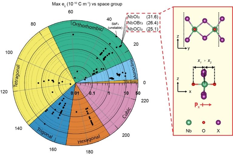
Figure shows (left) the sheet piezoelectric stress tensor elements computed for 2,940 different materials in their monolayer form. The maximum sheet piezoelectric stress tensor elements, eij, are plotted on a log scale in units of 10-10 C/m (radial axis), according to the space group (crystal structure) classification for the materials (angular axis). (Right) the atomic structure of NbOX2 (X = Cl, Br, I) shows a breaking of symmetry in the x-direction.
Reference: Wu, Y., Abdelwahab, I., Kwon, K.C. et al. Data-driven discovery of high performance layered van der Waals piezoelectric NbOI2. Nat Commun 13, 1884 (2022)
DOI: https://doi.org/10.1038/s41467-022-29495-y
Alignment of quantized levels in valleytronic materials
Featured in NUS News: https://www.science.nus.edu.sg/blog/2022/06/13/alignment-of-quantized-levels-in-valleytronic-materials/ (13 June 2022)
We have predicted that Landau levels belonging to different valleys in a two-dimensional (2D) valleytronic material, monolayer tungsten diselenide (WSe2), can be aligned at a critical magnetic field. Quantized electronic levels emerge when a magnetic field is applied to a 2D material. These levels are called Landau levels. Of particular interest are Landau levels in valleytronic materials. Valleytronic materials are materials in which one can control not just the charge or spin of an electron, but also the “valley” to which the electron belongs. In general, charge carriers in different valleys travel in opposite directions.
We have developed an approach to account for the effect of dynamical electron-electron interactions when predicting the energy levels in valleytronic materials in the presence of a magnetic field. Our predictions show that these many-body interactions amplified the effects of a magnetic field on the materials by causing a shift in their energy levels. When applied to monolayer WSe2, the computational results were found to be in quantitative agreement with experimental literature, validating the new approach.
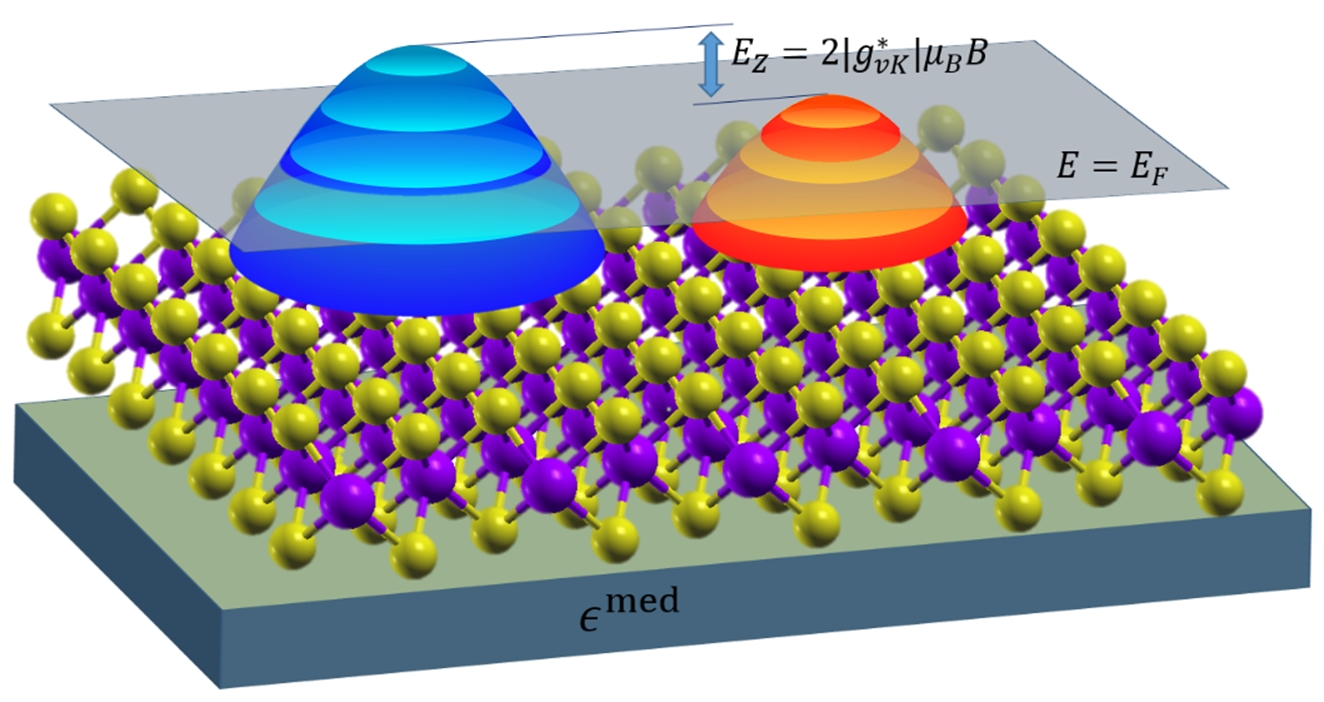
The figure above shows the Landau levels in doped monolayer WSe2, in response to an external magnetic field, B. The valleys are shown in blue and orange. The g-factor, g*vK, is enhanced due to dynamical many-body interactions arising from the change in carrier density in each valley, as the energy difference between the valley extrema, Ez, changes with B.
Reference: Xuan, F., Quek, S.Y. Valley-filling instability and critical magnetic field for interaction-enhanced Zeeman response in doped WSe2 monolayers. npj Comput Mater 7, 198 (2021)
DOI: https://doi.org/10.1038/s41524-021-00665-8
Layman's Introduction of Single Photon Emitters in Hexagonal Boron Nitride
Flying optical quantum bits, or qubits, play a crucial role in passing quantum information between different components of quantum computing and communication devices. One of the most important sources of optical qubits consists of single photon emitters (SPEs) in solid state materials. Recently, SPEs in two dimensional materials such as hexagonal boron nitride (hBN) have garnered significant attention. However, the exact relationship between the atomic structure of the defect centres and their photophysical characteristics is still largely missing. Using advanced first principles calculations, we elucidate the photophysical characteristics of six promising defect centres in hBN that can be intentionally created in experiments. We discuss the implications of our results on defect identification and fabrication, emission wavelength and polarization, optical addressability, and radiative decay rates.
See Reference: J. Phys. Chem. C, 125, 21791 (2021)
DOI: https://doi.org/10.1021/acs.jpcc.1c07729
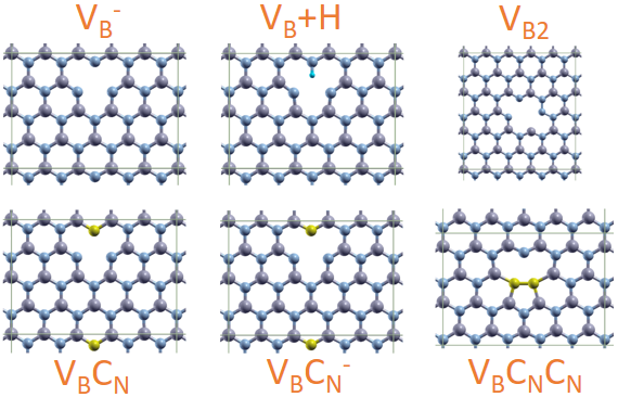
This figure depicts the periodic supercells of the six defect centres in the hexagonal boron nitride material investigated in our work, they are: VB−, VB+H, VB2, VBCN, VBCN− and VBCNCN.
Prediction of High Temperature Bose-Einstein Condensation of Excitons in Organic-2D Heterostructures
Featured in NUS News: https://www.science.nus.edu.sg/blog/category/research-news/ (06 December 2021)
A Bose-Einstein condensate is an extreme state of matter in which all particles have the same energy and are completely coordinated. The 2001 Nobel Prize in Physics was awarded for the realization of Bose-Einstein condensation. This phenomenal breakthrough was first achieved in a collection of rubidium atoms, at ultra-low temperatures of 20 nK.
We predict Bose-Einstein condensation (BEC) of charge transfer excitons can take place at ~50-100 K in systems of organic molecules on 2D semiconducting materials. This BEC temperature is orders of magnitude higher than that previously achieved in atoms. The narrow bandwidth of the molecular states also implies that the charge transfer excitons have very small momentum, thus favouring BEC.
Organic molecules such as transition metal phthalocyanines readily form ordered, self-assembled monolayers on 2D materials. The prediction of high temperature BEC of excitons in organic-2D material systems is expected to lead to more practical realizations of this exotic state of matter, and paves the way for the study of intriguing applications related to Bose-Einstein condensates.
![]()
Charge transfer excitons in organic-2D heterostructure: Schematic figure showing charge-transfer excitons in the ZnPc-MoS2 organic-2D heterostructure. The lowest energy charge transfer excitons in ZnPc/MoS2 heterostucture are predicted to undergo Bose-Einstein condensation at ~50-100K.
Reference: Ulman K; Quek SY, “Organic-2D Material Heterostructures: A Promising Platform for Exciton Condensation and Multiplication” NANO LETTERS 2021, 21, 8888−8894.
DOI: https://doi.org/10.1021/acs.nanolett.1c03435
Predictions of magnetic field response in 2D valleytronics materials
Featured in NUS News: https://www.science.nus.edu.sg/blog/category/research-news/ (08 September 2020)
We present a parameter-free approach to quantitatively predict the response of two-dimensional valleytronics materials to an external magnetic field. The predicted Landau levels match well to those deduced from recent optical experiments, and further demonstrate the importance of many-body interactions in determining the magnitude of the Zeeman effect in these systems.
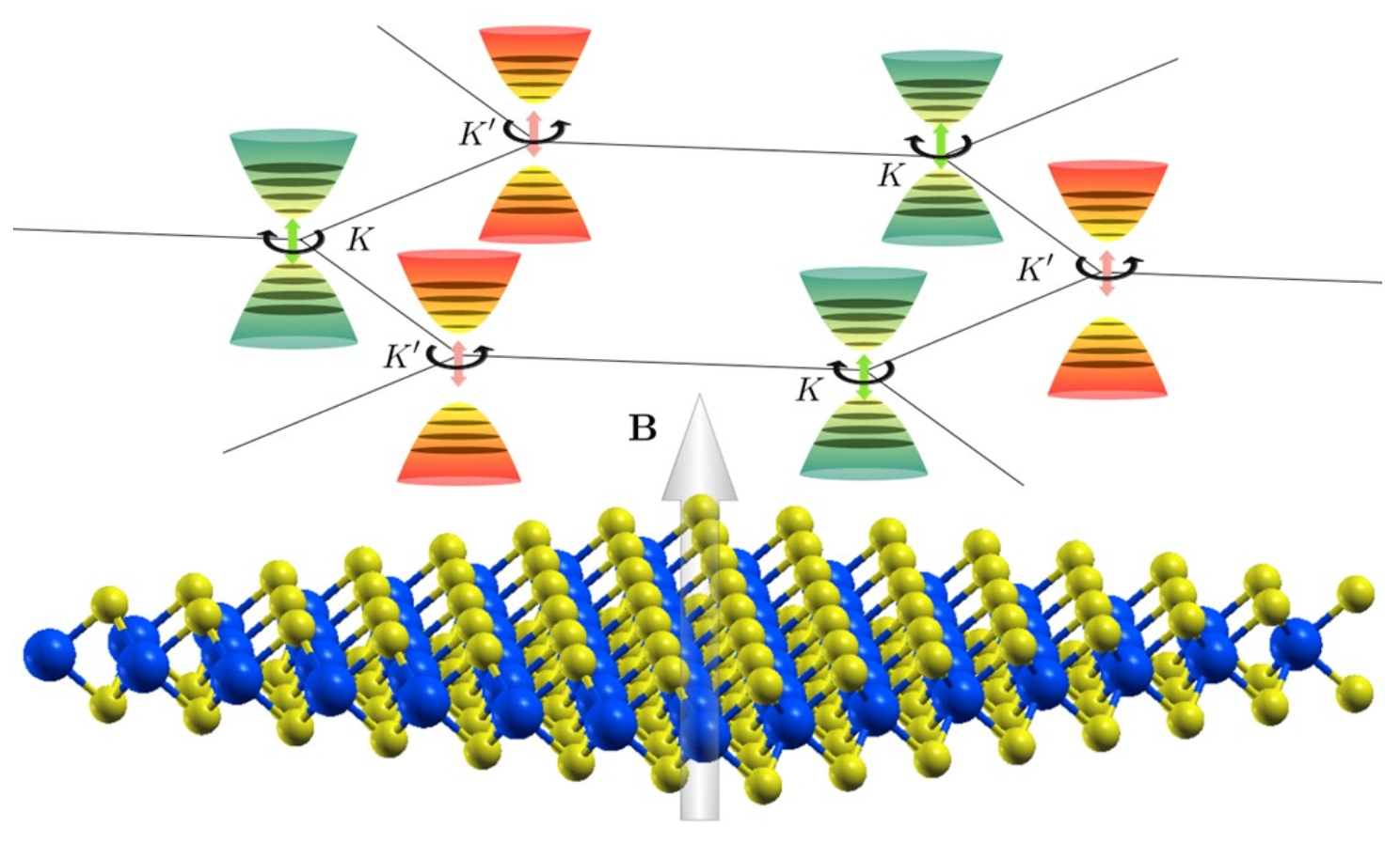
The figure shows the crystal structure of a 2D transition metal dichalcogenide (bottom) with the inequivalent valleys (K and K') representing the different momenta of electrons in the material (top). In the presence of a magnetic field (denoted by B), the energies of electronic states at the respective valleys are shifted by the Zeeman effect, and the states reorganise to form quantised Landau levels in each valley. Electronic states at each valley (orange and green) couple to light that is circularly polarised in one direction.
Stabilisation of charge density wave phase
by interfacial interactions
Featured in NUS News: https://www.science.nus.edu.sg/blog/category/research-news/ (22 July 2020)
In some low-dimensional materials, electrons form coherent, periodic waves in the crystal lattice,
resulting in wave-like distortions in the atomic lattice called a charge density wave (CDW) phase. The CDW phase can exhibit novel phenomena,
and has a different electrical conductivity from the usual phase which can potentially
lead to new advances in device applications.
A charge density wave (CDW) state is a macroscopic quantum state exhibiting periodic lattice distortion and a modulation of the electron density modulation,
leading to novel phenomena associated with these spontaneously broken symmetries. However, the CDW phase typically exists at very low temperatures.
Efforts to increase the CDW phase transition temperature, known as TCDW, have focused on the impact of interfacial strain and charge dopants.
However, the effects of such modifications on TCDW have not been significant, because the extent to which the CDW phase is stabilised by such modifications isintrinsically limited.
In this work, a room temperature CDW phase is stabilized in H-phase TaS2 bilayers when they are epitaxially grown on h-BN substrates. This phase was observed by our experimental collaborators led by Prof Loh Kian Ping in NUS. Using density functional theory calculations, we showed that the stabilization of the CDW phase was primarily due to the Moiré electrostatic modulation interactions at the TaS2/h-BN interface. Calculations on 18 different stacking configurations show that the tantalum (Ta) and S atoms are always arranged in such a way that the (+) group is centered on the underlying nitrogen (N) atom, while the (-) group is centered on the underlying boron (B) atom. This observation can be understood from the fact that the S atoms carry a slight negative charge in TaS2. They are repelled by the negatively charged N atom in h-BN, and attracted by the positively charged B atom. This novel mechanism for the stabilisation of the CDW phase is confirmed by the experimental observation that TaS2 randomly oriented on the h-BN substrate does not have a room temperature CDW phase.
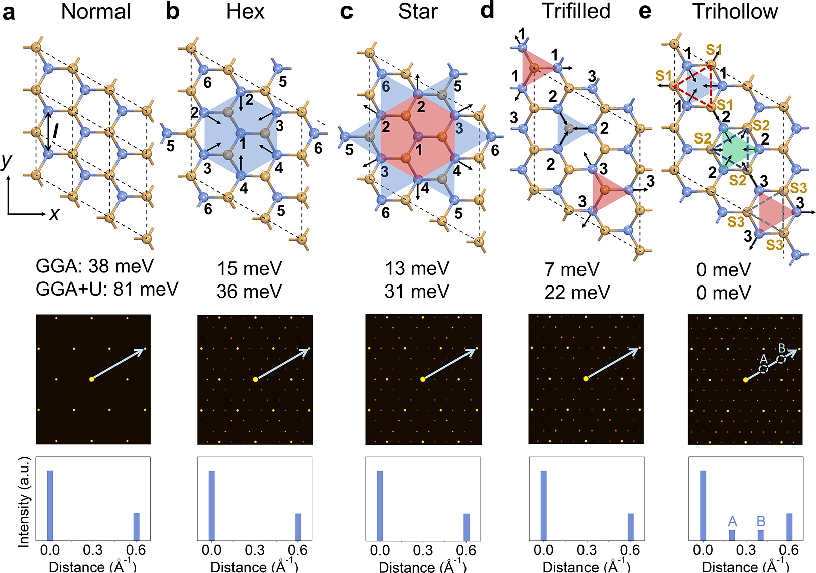
The figure shows the distortion of the tantalum for 4 different structures when placed over the h-BN substrate leading to the CDW
structures. Below these structures are the simulated FFT images.
Screening by 2D materials
Imagine wearing a wrist slap bracelet
which can emit light or store your personal data. Organic-2D material
hybrids present the next frontier of flexible electronic and optoelectronic
devices. The interfacial energy-level alignment plays a major role in the
operation of such devices. A key theme of our present research is to
understand how electronic screening by 2D materials at these novel hybrid
interfaces changes the energy-level alignment of adsorbed organic molecules,
which determine the tunneling barriers faced by electron and hole carriers
at the organic-2D material interface.
Electronic screening is a process in
which the electrons in a material rearrange themselves under the application
of an external electric field. Being atomically thin, electronic screening
within a 2D material is known to be significantly weaker than a bulk
material. The screening of charges adjacent to a 2D material,
however, is different. Using first-principles calculations, we found that
just a single layer of a 2D material is able to significantly impact the
energy levels of an organic molecule placed above it. In fact, a 2D material
can screen just as effectively as a 3D one with the same energy gap. This
result shows that electronic screening by 2D materials is non-trivial and
needs to be carefully investigated in consideration of designing
next-generation electronic devices.
Hexagonal boron nitride, a 2D material,
has been demonstrated to be an excellent substrate for graphene-based
electronics by significantly reducing charge inhomogeneities above it. With
our first-principles calculations, we provide evidence that, in general, 2D
materials can serve as excellent substrates due to their intrinsic ability
to screen out the effect of charge impurities beneath them. (This insight
would have been difficult to probe within a laboratory where environmental
effects would have to be taken into account.)

The figure shows the induced screening charge (blue: depletion of electron
charge; red: accumulation of electron charge) due to a point electron charge
perturbation located on the benzene molecule, which is adsorbed on a
hexagonal boron nitride monolayer substrate.
Localized excitons in 2D
materials for integrated quantum optics
Featured in NUS News: https://news.nus.edu.sg/research/infocus (22 July 2019)
We have unveiled the nature of point
defects and localized excitons in tungsten diselenide (WSe2)
single layers for novel integrated quantum optical applications.
Two-dimensional (2D) material
systems have recently been found to host localized excitons and single
photon emitters (SPEs), meaning that light is emitted from colour centers
one photon at a time. This has huge implications in quantum optics and
quantum information processing, where device integration and up-scaling are
currently the biggest challenges to surmount. SPEs in 2D materials such as
WSe2, are intrinsically embedded in a two-dimensional material
matrix, allowing for potential device and circuit integration as in
conventional semiconductor industry. However, the detailed nature of these
experimentally discovered SPEs in WSe2 are still unknown, which
hinders their further utilization and application. We have now unveiled the
nature of point defects and localized excitons in WSe2 single
layers through a combination of theory and experiment.
To exactly pin-point the SPE-related
point defects and correlate their nature with the corresponding emission
line is a non-trivial task. For the well-established single photon quantum
emitters in diamond systems, researchers took decades to finally ascertain
the exact energy level structure of the exact defect centers responsible for
the SPE in diamond. Similarly, the chemical origins and detailed energy
levels of defect centers responsible for SPEs in 2D materials have been
controversial so far. The difficulty arises from several different
perspectives. The spatially resolution of experimental characterization
techniques has not reached single atomic limit, when the photo-activities of
those sites need to be determined simultaneously. On the other hand,
theoretical descriptions of defect centers are usually quantitatively
unsatisfactory or inconclusive.
Here, our group has studied
theoretically the point defects and localized excitons in a 2D WSe2,
in collaboration with our experimental collaborators, Professor Andrew Wee
and Professor Stephen Pennycook in NUS. We first conducted exhaustive
density functional theory (DFT) calculations on intrinsic point defects in
WSe2. The experimental scanning tunneling microscopy and
spectroscopy (STM/S) methods are used to characterize the most abundant
point defects in the same system. It was found that none of the intrinsic
point defects in the system matches the experimental STS spectra. Thus, the
researchers then focused on the oxygen-related point defects of WSe2,
which they found could be incorporated easily into the material
inadvertently, either during the synthesis process or by ambient
passivation. Through comparison of experimental and simulated STM images,
the researchers identified oxygen substituted Se vacancies (OSe)
and oxygen interstitials in the lattice (Oins) as the most
abundant point defects in WSe2. Additionally, scanning
transmission electron microscopy (STEM) images identified an additional SeW
anti-site defect. Subsequently, state-of-the-art many body perturbation
theory based GW-Bethe Salpeter equation (GW-BSE) calculations are conducted
for the three most likely extrinsic defects identified in WSe2:
OSe, Oins and SeW. It was
found that only the Oins defect hosts localized
exciton states close to the experimentally observed spectral positions. OSe
does not possess localized excitons, while SeW has localized
excitons too low in energy. The mechanical strain gradient within the
material will also help to tune the spectral position and funnel excitons
into the bottom of the strain well.
This work presents a detailed study
of point defects in monolayer WSe2 and predicted the nature and
energies of excitons at these defect sites. The implications of the
experimentally observed point defects on the optical response have been
predicted. The key point here is that of all the experimentally observed
point defects, only one candidate (Oins) is available that gives
localized excitons in the energy range observed in recent SPE experiments.
These predictions suggest ways to create quantum emitters in other
semiconducting TMDs, e.g., through controlled reaction with O2,
as well as their further integration into quantum optical applications.

Figure shows experimentally observed
Oins point defect STM image, in comparison with DFT simulated
counterpart. The GW-BSE optical absorption spectrum together with labeled
localized excitons (LXs) are displayed on the top right panel. A schematic
of the effects of strain gradients is shown on the bottom right panel.
Tunneling Barriers at Large Interface Systems from Many-body Perturbation Theory: the XAF-GW method
Many-body perturbation theory in the
GW approximation can give accurate quasiparticle levels for the electrons
and holes, and therefore accurate energy barriers. However, the conventional
GW code is limited to rather small systems due to high computational cost
and memory. One key bottleneck is the computation of the polarizability
(chi) matrix. Several groups have simplified the computation of chi for
interfaces with no hybridization, by taking the chi matrix for the full
system to be the sum of the chi matrices of the individual components.
However, it is often assumed that this method breaks down in the presence of
hybridization between the individual components.
In our group, we have developed a
method, which we call XAF-GW (X: eXpand-chi, A: Add-chi, F: Full
wavefunctions), that enables GW calculations for large interface systems. We
show analytically that even in the presence of interface hybridization to
form bonding and anti-bonding states, the chi matrix of the full interface
is still a sum of the individual components, up to first order in the
overlap matrix elements involved in the hybridization. The approach is
validated by showing that the band structure obtained using this method is
almost identical to that obtained using a regular GW calculation for bilayer
black phosphorus, where interlayer hybridization is significant. Significant
savings in computational time and memory are obtained by computing chi only
for the smallest sub-unit cell of each component, and expanding (unfolding)
the chi matrix to that in the unit cell of the interface. To treat interface
hybridization, the full wavefunctions of the interface are used in computing
the self-energy.
Using this approach, we have
successfully obtained accurate quasiparticle levels and energy barriers for
an experimentally relevant organic/2D material system, as shown in the
figure below.
The XAF-GW approach is easy to
implement and will enable accurate prediction of quasiparticle levels and
energy barriers at large interface systems, including other organic/2D
material interfaces, and twisted bilayer systems.

FIG. PTCDA on monolayer WSe2
supported on bilayer graphene. (a) Side view of atomic structure. (b) Top
view showing WSe2 monolayer in one unit cell of the
heterostructure. The green box indicates the sub-unit cell used for
computing the chi matrix of WSe2. (c) Computed projected density
of states (PDOS) for PTCDA on WSe2/bilayer graphene. Red: XAF-GW,
Blue: DFT, (d) Experimental scanning tunneling spectroscopy (STS) spectrum
for PTCDA on WSe2/Graphite from ACS Nano 10, 2476 (2016). The
levels of the HOMO (highest occupied molecular level) and LUMO (lowest
unoccupied molecular level) predicted using XAF-GW agree well with those
measured in the STS spectrum.
Energy level alignment for molecular electronics
13 Mar 2018. NUS physicists have found that complex electron-electron interactions change the energy levels at molecule-metal interfaces, affecting the performance of molecular electronic devices.
Molecular electronics involves the use of molecules as the main building block for creating the electronic circuitry. It can potentially be used to develop circuits that are much smaller than those made from conventional silicon processes. Understanding the electronic properties of the interface between the molecules and metal conductors, particularly their associated energy levels, is important for rationalising and optimising device performance. This is central to the development of molecular electronics.
A fundamental property of every molecule is its energy gap, defined as the energy difference between the highest and lowest orbital energy level occupied and unoccupied by electrons respectively. These levels are also the most important energy levels for device performance. The energy gap of a molecule becomes smaller when the molecule is brought close to a metal surface; this will make it easier for charge carriers to move between the molecule and the metal contact. This change in gap is primarily caused by electronic screening effects from the metal surface, and can be as large as several electron-volts. However, this electronic screening effect is missing from the majority of theoretical studies on this topic.
A research team led by Prof Su Ying QUEK, from the Department of Physics, NUS has elucidated the interface electronic structure properties for a number of different molecules on gold surfaces using state-of-the-art theoretical and computational methods that explicitly take into account electronic screening effects from first principles. The researchers carried out computations on molecular systems anchored by common chemical functional groups (amine, pyridine and thiolate groups). The research team found that for a single molecule, the electronic screening effect can be accurately predicted from an image charge model, even in the presence of chemical bonds. The image charge model is a classical electrostatics method which approximates the electronic screening of a test charge by an image charge in the metal. However, in devices with many molecules, the researchers found significant additional electronic screening mechanisms. Besides intermolecular screening effects, substrate-mediated intermolecular interactions are also found to contribute to these additional screening mechanisms. The findings suggest that charge carriers can tunnel more easily across the interface in devices with many molecules.
Prof Quek said, “This work provides valuable insights into the many electron effects at the molecule-metal interfaces involving chemical bonds. The results and findings from this research constitute an important step towards the understanding and manipulation of functional organic systems in the development of molecular devices.”
See Reference:
The Journal of Physical Chemistry C 121, 13125 (2017)

(Left) Figure shows the electron energy level alignment of benzene-diamine
molecules on gold surface system (shown on the right). The energy levels are
shown for a molecular layer (black) and for a single molecule (red). (Right)
Illustration of the benzene-diamine molecules on gold surface.
A new spin on graphene electronics
18 May 2017. NUS physicists have discovered that controlling electron spin can lower contact resistance in graphene electronics for high performance devices.
Electronic devices with lower resistance between connections uses less power. These devices are also less likely to have localised heating effects. Graphene, a flexible material with exceptionally high electron mobility and thermal conductivity, is a material for next generation electronics. However, it has a large resistance when used in electrical connections. The construction of smaller and more efficient electronic devices is hindered partly by heat generated within the device. If this resistance can be lowered, electronic devices will be able to operate at a higher speed using less power. An NUS team has now shown how the contact resistance can be reduced in graphene devices by manipulating the spin state of the charge carriers.
Although graphene is a prime candidate material for next generation electronics the large electrical resistance at metal-graphene interfaces is a bottleneck for practical devices. A collaboration between Prof Su Ying QUEK from the Department of Physics, NUS and Prof John THONG from the Department of Electrical and Computer Engineering, NUS has shown that “edge-contacted” device geometries in Ni/Co-graphene interfaces result in some of the lowest contact resistances reported to date. The resistance in such geometries is significantly lower than in “surface-contacted” Ni/Co-graphene interfaces. This is due to the different behaviour of electron spins in these geometries. Temperature-dependent measurements show that electron spin indeed can control the contact resistance at ferromagnetic-graphene interfaces.
There have been significant efforts in graphene research due to its unique material properties including high electron mobility, excellent mechanical strength and flexibility, and high thermal conductivity. This has prompted the use of graphene as a potential material for on-chip interconnects and high-speed transistors for next generation electronic circuits. However, the large electrical resistance at the metal-graphene interface limits the performance of these devices.
In this work, the researchers examined the contact resistance of edge- versus conventional surface-contacted ferromagnetic metal-graphene interfaces. They found that the contact resistance of edge-contacted interfaces is much lower, with resistances comparable to the lowest values reported to date. They showed that the higher contact resistance arises from the spin filtering phenomena at the metal-graphene interface. This is in contrast to previously reported work, where it is widely believed that the higher resistance is a result of weaker coupling strength. By using edge contacts, one essentially allows charge carriers of both majority and minority spin to pass from the electrodes to graphene, resulting in almost twice the number of carriers and reducing the contact resistance significantly. These findings suggest that the contact resistance in graphene devices could be adjusted by tuning the spin state of the magnetic metal.
The research team plans to explore tuning the contact resistance in ferromagnetic metal-graphene contacts by varying the spin state of the metal. They also intend to investigate other device parameters such as spin injection efficiency and spin lifetime at these interfaces for spintronics applications.
See reference:
ACS Nano 10, 11219 (2016)

Figure shows the schematic for edge- and surface-contacted ferromagnetic
metal-graphene interfaces with spin-up and spin-down current flows denoted
by blue and red arrows, respectively.
Interlayer interactions and Electrically-Tunable Dirac Cone in Few-layer Black Phosphorous
Black Phosphorus is a recently isolated 2D material that, like graphene, consists of only one element. Black Phosphorus has attracted tremendous interest due to its very high carrier mobility that is as good as that in silicon. Interestingly, unlike many other 2D materials, the interlayer interactions are not of purely van der Waals type. We show, with our experimental colleagues, that the interlayer interactions in black phosphorus are substantially larger and of significant covalent nature.
See Reference: Nano letters 15, 3931 (2015)
We also predicted that the application of an external electric field can result in a tunable Dirac cone in few-layer black phosphorus. This prediction was later verified in experiments in this recent Science article.
See Reference: Scientific Reports 5, 11699 (2015).

Flexible electronics and optoelectronics from 2D materials

Transition metal dichalcogenides (TMDs) MX2 (M=Mo, W, etc.; X=S, Se, or Te;) are a class of layered structure materials that received enormous attention recently for potential promising applications. Like 2D graphene or boron-nitride, they can also be exfoliated into single or few layer films from bulk or synthesized bottom-up from chemical vapor deposition (CVD) or molecular beam epitaxy (MBE) methods. Unlike graphene or boron-nitride, 2D TMDs have semiconducting band gaps at about 1.0~2.0 eV, ideal for electronics and optoelectronics applications. Moreover, these ultra-thin semiconducting films are super-flexible and super-robust in mechanical elasticity. They are found to endure very large strain of 10-20%, allowing for possibilities of flexible device applications. Recently, in collaborating with experimentalists, we identify a unique band gap modulation behavior of CVD-grown 2D MoS2 monolayers across its grain boundaries (GBs); see the figure above. We attribute it to a superposition of strain field modulation near the GBs together with defect-induced band bending near the dislocation core of the GBs. These findings offer us knowledge about and insights into electronic properties of 2D TMD monolayers and paves the way for further engineering possibilities.
See Reference: Nature Communications 6:6298 (2015).
Contact Resistance in MoS2 transistors
Besides being of fundamental interest, our work also has applications in the realm of engineering. We study the Schottky barriers and contact resistances to different 2D materials. In this recent work, we work with our experimental collaborators to show that the insertion of a graphene interlayer significantly reduces the contact resistance in Nickel-MoS2 field effect transistors.See Reference: ACS Nano 9, 869 (2015)

More than skin-deep
6 Sep 2014. NUS researchers discovered that stronger surface bonds have non-trivial effects on the natural frequencies in 2D systems.
Few of us have gone through childhood without the unpleasant experience of our skin peeling off after an injury. In the world of materials science, the tiny atoms that make up a material generally experience significant grief when they lose a few of their neighbors through the creation of a surface. These surface atoms start to gravitate more strongly towards their remaining neighbors, sometimes resulting in beautiful atomic-scale rearrangements.
Two-dimensional (2D) layered materials have taken the world of materials science by storm. Unlike other materials, one would expect that peeling off layers to create a surface in a layered material should not cause much grief to the surface atoms. A team led by Prof QUEK Su Ying from Department of Physics in NUS has found, however, that even in layered materials, surface atoms feel the loss of the missing neighboring layer enough to cling on more strongly to their remaining neighbors in the same layer. And these stronger surface interactions account for previously unexplained anomalous trends in the vibrational frequencies of these prototypical 2D materials.
Vibrational frequencies are routinely used to identify the thickness of 2D materials. For the vibration which involves adjacent layers moving against one another (see Figure). It was thought that the frequency should increase with thickness due to increased friction in thicker materials. By parameterizing high-level calculations into a simple physically-motivated model, the team found this to be indeed the case if the surface force constants are the same as in the bulk material. However, once the stronger surface force constants are accounted for, the frequency decreases with increasing thickness, in excellent agreement with experiments. Similar effects have since been found in other 2D layered materials.
These findings change the mindset that surface effects are not important in layered materials, and have implications for predicting vibrational frequencies and thermal properties in these systems.
See References: Physical Review B 88, 075320 (2013), Nano Letters 13, 1007 (2013), Critical Reviews in Solid State and Materials Sciences 39, 319 (2014)
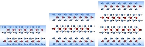
Image shows vibrations in 2 layered, 3 layered and 4 layered 2D MoS2. Molybdenum atoms (red spheres) and Sulphur atoms (blue spheres) are bonded together by strong bond within each layer, but adjacent layers interact weakly. The blue shading in the background indicates the surface region where intralayer bonds are strengthened. (Image credit: LUO Xin and QUEK Su Ying)
Raman Spectra in 2D materials
A photon incident on a material can result in the emission or absorption of a phonon (collective lattice vibration) that changes the frequency of the emitted photon. This Raman process, the subject of the 1930 Nobel Prize in Physics, provides a non-destructive and sensitive tool to probe the phonon spectra in materials as well as provide a fingerprint to identify the material in question. We have ongoing collaborations with experimental groups to understand the Raman spectra in 2D materials.Our theoretical findings, such as the importance of surface effects on the phonon frequencies have also been adopted by other groups.

Above: Interlayer shear and breathing modes in 2D MoS2 (experiment versus theory) Nano Letters 13, 1007 (2013)