Research
We are interested in electronic, optoelectronic, and spintronic phenomena that are unique to van der Waals materials and their heterostructures, especially in the atomically thin limit where dimensionality plays a fundamental role in defining the material properties. Many chemical compounds and elemental substances naturally crystallize in a van der Waals layer structure that can be thinned down to mono- to few-layer crystals that are no more than a few atoms thick and effectively two-dimensional (2D). Due to distinct symmetry, reduced screening, and quantum confinement, 2D materials exhibit a unique set of physical properties that are absent in traditional materials and offer fertile ground for developing next-generation technologies. Condensed matter phenomena intrinsic to these materials are key to addressing interesting questions associated with many-body physics and topological nature of electronic states. We experimentally explore such questions with a view to developing novel applications in energy, computation, and communication.
Exciton quantum photonics
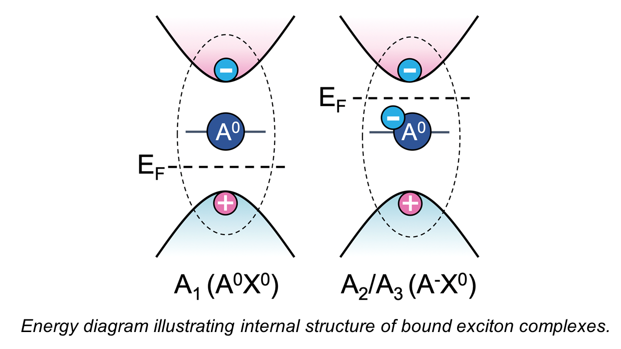
Atomic defects in semiconductors can act as optically addressable luminescence centers that can serve as a building block in solid-state quantum technology such as single photon emitters and qubits. Unlike color centers in insulators where optical transitions mainly involve atom-like defect states, defect emission lines in semiconductors are often attributed to bound exciton complexes - many-body particles retaining some free exciton character. The electron spin of the defect in the complexes can act as long-lived qubit with long spin coherence, making them attractive for quantum memory devices. In traditional semiconductors such as GaA, however, distinct features of these complexes are only observable at cryogenic temperatures (< 20 K) due to their small binding energies, limiting their applications. Atomically thin group 6 transition metal dichalcogenides (TMDs) are direct band gap semiconductors with strong excitonic character. TMDs host a variety of exciton species, many of which are observable at room temperature due to their large binding energies. Theory has predicted that 2D TMDs can also host a variety of bound exciton complexes that are stable at room temperature. Different bound exciton complexes are expected to exhibit distinct properties due to the different degrees of freedom of the component particles. We aim to develop quantum photonics elements based on 2D semiconductors by atomic defect engineering and spectroscopic investigation of bound exciton complexes.
• Z. Zhang et al. “Optically Active Chalcogen Vacancies in Monolayer Semiconductors” Adv. Opt. Mater. 2201350 (2022).
• L. Loh et al. “Impurity-Induced Emission in Re-Doped WS2 Monolayers” Nano Lett. 21, 5293 (2021).
Electrically tunable magnetism
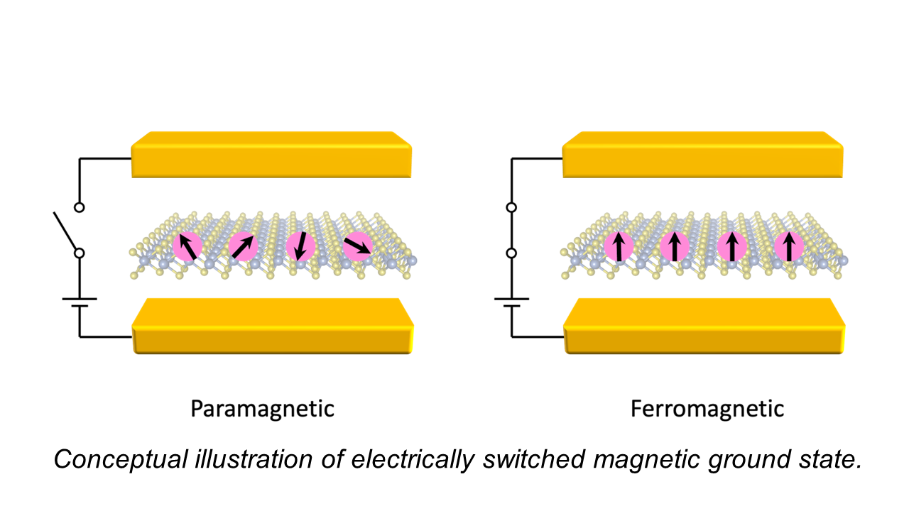
Electrical control of magnetic order is a long-standing challenge in the development of spintronics. The ability to alter the magnetic ground state of a material in a manner similar to electrical gating of charge current is highly desirable for low power logic and memory operations. The aim is to achieve modulation of the magnetic exchange coupling as well as magnetization of a material in absence of either spin or charge current that results in undesirable energy dissipation. Recent observation of magnetic order in van der Waals materials in the ultrathin limit brought to light a number of attractive candidates for the study of electrically tunable magnetism. Among many remarkable features, of particular note is the unusual susceptibility of van der Waals magnetic materials to electrostatic fields with their Curie temperature electrically tunable over a wide temperature range. We recently discovered that electrochemical doping of Cr2Ge2Te6 results in remarkable enhancement of the Curie temperature by 150 K accompanied by a change the sign of magnetic anisotropy energy. We investigate the underlying mechanism of such behaviors and aim to achieve energy-efficient spintronic logic and memory devices.
• I. Verzhbitskiy and G. Eda “Electrostatic control of magnetism: Emergent opportunities with van der Waals materials” Appl. Phys. Lett. 121, 060501 (2022).
• I. Verzhbitskiy et al.“Controlling the magnetic anisotropy in Cr2Ge2Te6 by electrostatic gating” Nature Electronics 3, 460 (2020).
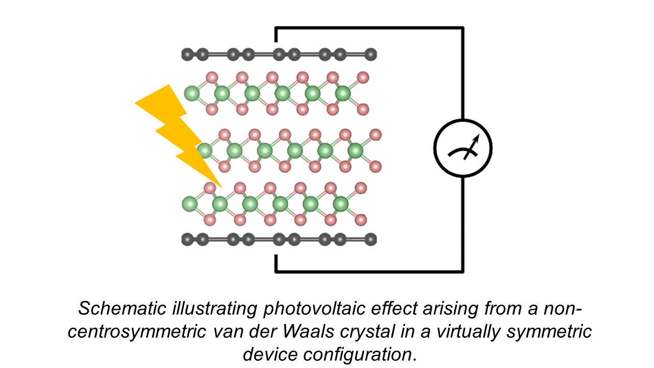
Bulk photovoltaic effect
Symmetry is a fundamental material property that defines the response of a material to external stimuli. Bulk photovoltaic effect is a peculiar phenomenon that occurs when light interacts with a crystal with broken inversion symmetry. This effect arises from coherent quantum mechanical motion of photoexcited carriers and results in steady-state charge (or spin) current. Bulk photovoltaic effect is expected to offer advantages for energy harvesting and sensing over traditional junction-based devices due to robust coherent transport of photocarriers. For example, shift current, which is one of the representative mechanisms of bulk photovoltaic effect, is insensitive to defects due to its topological origin. Van der Waals materials are an excellent platform for the fundamental investigation of such topological photocurrent due to their remarkable amenability for symmetry engineering. We aim to unravel the mechanisms of bulk photovoltaic effect and identify solutions for its practical applications.
Quantum materials sysnthesis
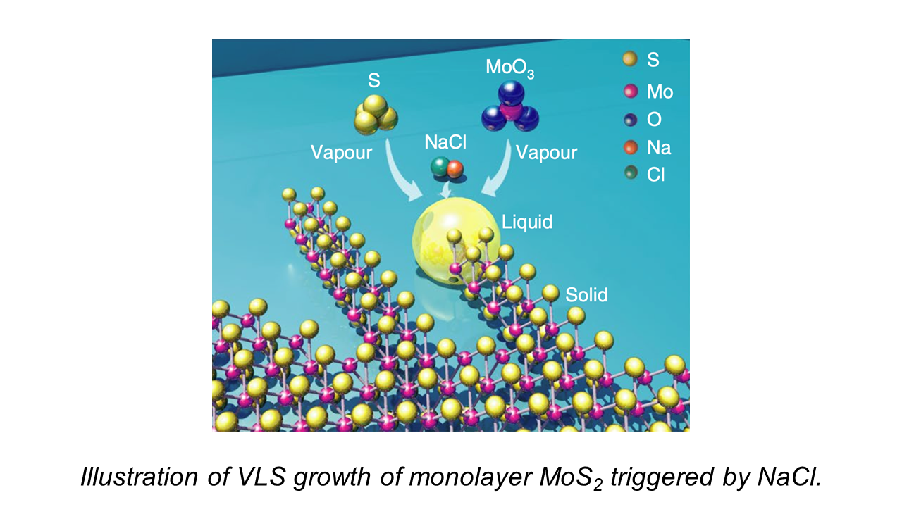
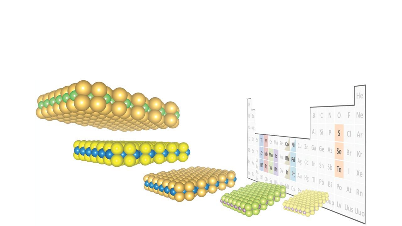
Fundamental physical and chemical properties of a given material depends not only on its chemical composition but also on the microscopic details of its crystal structure. Van der Waals materials occur in various polytypes and polymorphs and each of them exhibits distinct properties due to its unique symmetry and electronic energy dispersion. The ability to synthesize materials with a specific crystal structure is crucial to enable observation of novel condensed matter phenomena and unlocking new technologies. We aim to develop synthesis methods that allow controlled growth of van der Waals materials and their heterostructures with a desired crystal structure. We are particularly interested in the vapor-liquid-solid (VLS) mode of chemical vapor deposition that was developed in our lab in 2018. This method utilizes molten salt of precursors to trigger epitaxial growth of thin films and one-dimensional nanostructures at reduced temperatures. We aim to understand the principle of the epitaxial VLS growth and explore its applicability to a wide variety of quantum materials.
• Z. Qin et al. “Growth of Nb-Doped Monolayer WS2 by Liquid-Phase Precursor Mixing” ACS nano 13, 10768 (2019).
• S. Li et al. “Vapor-liquid-solid growth of monolayer MoS2 nanoribbons” Nat. Mater. 17, 535 (2018).