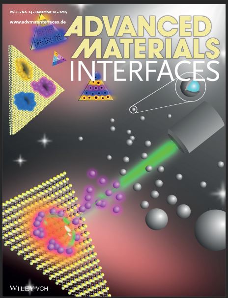
 "Laser-Guided Microcanvas Printing of Multicolor Upconversion Nanoparticles on Molybdenum Disulfide Monolayer", Adv. Mater. Interfaces, 6, 1901673, 2019
Scanning focused laser beams incident on nanomaterials have provided
a nondestructive and facile technique to fabricate micropatterns of a wide
variety of hybrid materials. Conventionally, the technique is limited to localized
chemical modification or in situ reduction of specific metal ions en route to
heterogeneous material systems. However, as hybrid structures continue to
be an essential form to couple various material properties and bring forth
nanostructures with designable traits, the need for a flexible technique to
interface nanomaterials presynthesized in higher quality remains an important
challenge. Herein, a technique for laser-guided microcanvas formation by
anchoring preformed upconversion nanoparticles at specific sites on a MoS2
monolayer surface is presented. The technique expands the building blocks
in laser-produced hybrid structures to include presynthesized nanomaterials.
The upconversion microstructures are formed via a microbubble-assisted
mechanism, with distinct emission contrast against the background. The
proof-of-concept production of a multicolor upconversion microcanvas marks
the potential for full-color high-resolution displays while the technique opens
up the possibility of fabricating an expandable range of new hybrid structures.
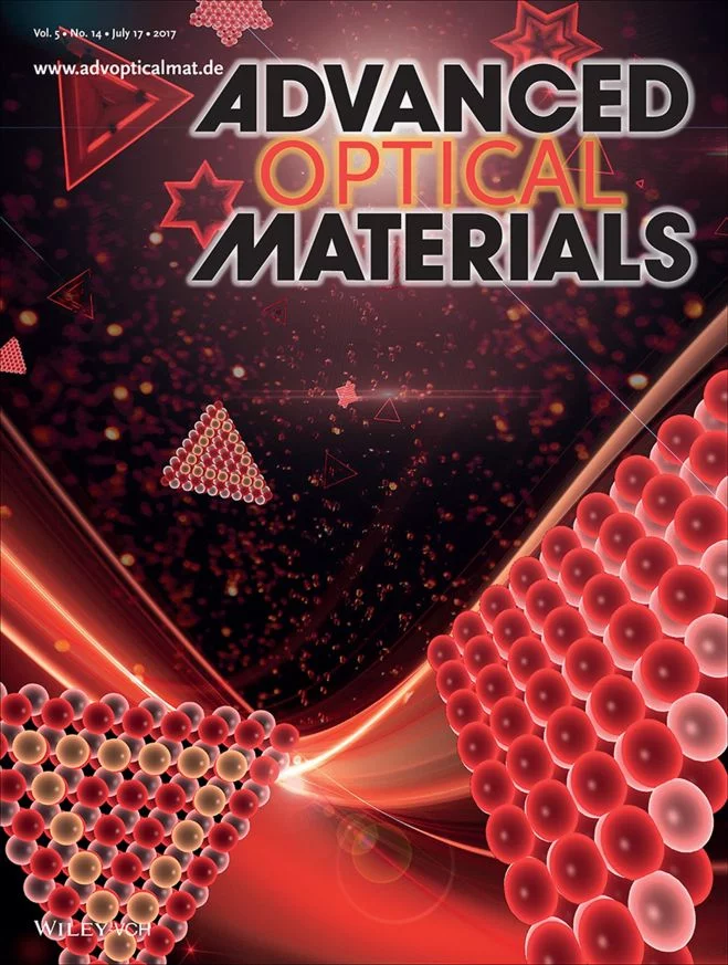 "Enriched Fluorescence Emission from WS2 Monoflake Empowered by Au Nanoexplorers", Adv. Opt. Mater., 5, 1700156, 2019
Gold nanoparticles (Au NPs) are deposited on monolayer 2D tungsten disulfide (WS2) microflake (monoflake) to probe the effects of gold deposition on the physical and chemical properties of the WS2 transition metal dichalcogenides. It is found that the Au NPs behave like nanoexplorers that map out subtle and hidden chemical heterogeneity within the WS2 monoflake by way of site-selective decoration on the WS2 monoflake. The resultant decorated Au NPs patterns trace the concentric fluorescence pattern found on the WS2 monoflake. The Au NPs enhance the fluorescence intensity in selected regions within the WS2 monoflake and even activate fluorescence emission from previously dark regions. Most remarkably, the photoluminescence spectra from WS2 with Au NPs are sharpened and dominated by neutral excitons. This is in stark contrast to photoluminescence emission from pristine WS2 monoflake where the spectrum exhibits a multitude of emissions from trions, biexcitons, neutral excitons, and defect-bounded excitons.
 "Defect Heterogeneity in Monolayer WS2 Unveiled by Work Function Variance", Chem. Mater., 31, 7970, 2019
Defects are commonly found in two-dimensional (2D) transition-metal dichalcogenide (TMD) materials. Such defects usually dictate the optical and electrical properties of TMDs. It is thus important to develop techniques to characterize the defects directly with good spatial resolution, specificity, and throughput. Herein, we demonstrate that Kelvin probe force microscopy (KPFM) is a versatile technique for this task. It is able to unveil defect heterogeneity of 2D materials with a spatial resolution of 10 nm and energy sensitivity better than 10 meV. KPFM mappings of monolayer WS2 exhibit interesting work function variances that are associated with defects distribution. This finding is verified by aberration-corrected scanning transmission electron microscopy and density functional theory calculations. In particular, a strong correlation among the work function, electrical and optical responses to the defects is revealed. Our findings demonstrate the potential of KPFM as an effective tool for exploring the intrinsic defects in TMDs.
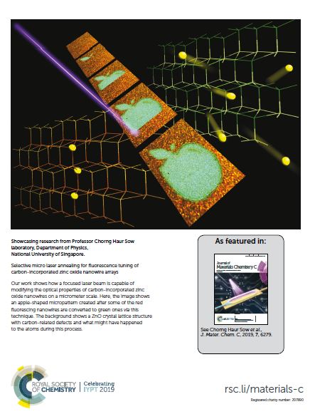 "Selective micro laser annealing for fluorescence tuning of carbon-incorporated zinc oxide
nanowire arrays", J. Mater. Chem. C, 7, 6279, 2019
"Selective micro laser annealing for fluorescence tuning of carbon-incorporated zinc oxide
nanowire arrays", J. Mater. Chem. C, 7, 6279, 2019
Carbon-incorporated zinc oxide (C-ZnO) nanowire (NW) arrays display controllable optical changes after being selectively annealed by a focused violet laser beam. A blue shift in the photoluminescence of the
NWs from orange to green emission with enhanced optical intensity is observed. Systematic studies of C-ZnO NW modification with varying laser powers, scanning speeds and surrounding oxygen concentrations
demonstrate a correlation between the oxygen concentration during laser annealing and the resultant extent of photoluminescence intensity change. Micro laser annealing and X-ray photoelectron spectroscopy as well
as electron microscopy experiments point to a mechanism involving the segregation of carbon species to the
NW surface followed by formation of zinc carbonate species on the NW surface. The work also provides
further evidence of the miscibility of carbon in ZnO and the existence of carbon-based defects during ZnO
NW growth.
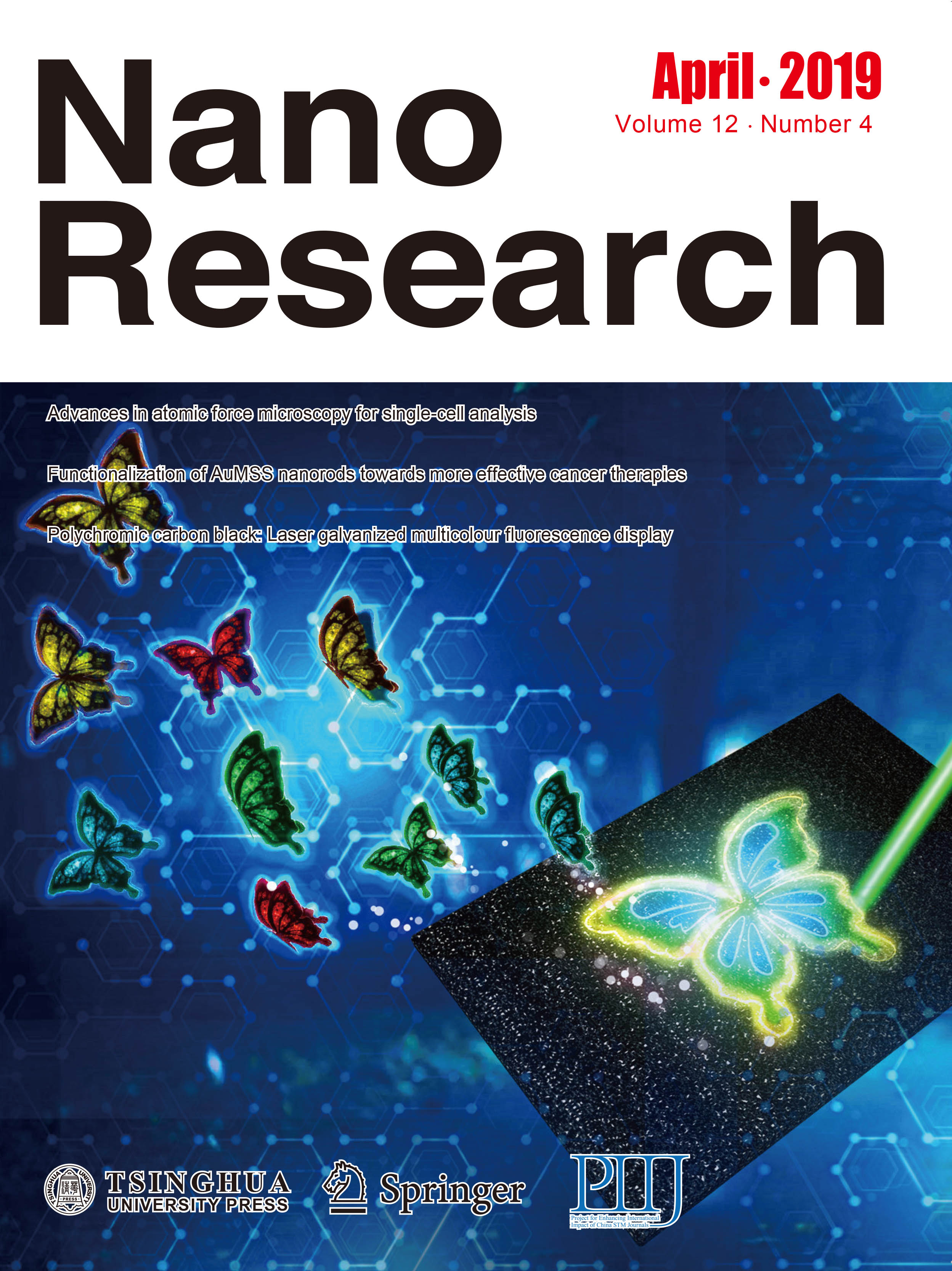 "Polychromic carbon black: Laser galvanized multicolour fluorescence display", Nano Research, 12, 733-740, 2019
Recovered carbon black (rCB), a very economical and abundance source of material, is transformed into dazzling multicolour fluorescence and visual display for the first time by way of a scanning focused laser treatment. This laser-initiated process is both straightforward and versatile, catering to both micro- and macro-scopic patterning with the sample in ambient or helium environment. The observed phenomenon is attributed to both chemical and structural induced colouration of rCB powder. Chemically, carbon infusion of oxidised metal occurs when photothermal reaction takes place in ambient. After laser modification with the sample in helium environment, the powder not only fluoresces due to sulphur impurities, control annealing of these powders results in formation of periodic arrangements of carbon nanoparticles. The periodicity of these arrangement falls within the range of visible wavelength, hence contributing to the visually observable rainbow coloured rCB flakes. The patterned sample is also transferrable using PDMS stamps. This in turn broadens the application of this material in flexible electronic devices/displays. Photocurrent measurements show most significant enhancement under yellow light illumination. Furthermore, in the presence of an applied potential, the fluorescence detected from the sample can easily be switched off. All in all, we present a simple process to add multiple functionalities to a material that is both inexpensive and sustainable.
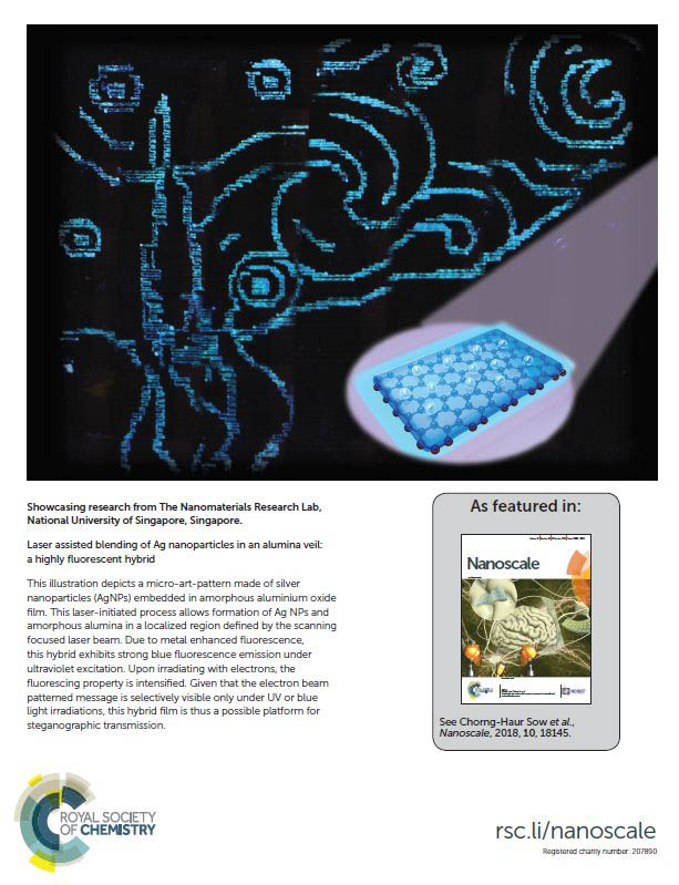 "Laser assisted blending of Ag nanoparticles in an alumina veil: a highly fluorescent hybrid", Nanoscale, 10, 18145-18152, 2018
We report a functional hybrid made of silver nanoparticles (AgNPs) embedded in an amorphous aluminium oxide (alumina) film. This laser-initiated process allows formation of AgNPs and amorphous alumina in localized regions defined by the scanning laser beam. Due to metal enhanced fluorescence, this hybrid exhibits strong blue fluorescence emission under ultraviolet excitation. Upon irradiating with electrons at dosages of 1 to 20 mC cm-2, AgNPs become more metallic while the Al film is further oxidised. As a result, the fluorescing property is intensified. Using a hybrid irradiated with 10 mC cm-2, the electronic conductivity of the sample is improved by 11.5 times compared to that of the as-synthesized hybrid film. Excitation by UV light on the sample results in an increase in the detected current of nearly 29 times. Given that the electron beam patterned message is selectively visible only under UV or blue light irradiation, this hybrid film is thus a possible platform for steganographic transmission.
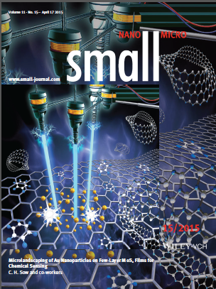 "Microlandscaping of Au Nanoparticles on Few-Layer MoS2 Films for Chemical Sensing", Small, 11, 1792-1800, 2015
Surface modification or decoration of ultrathin MoS2 films with chemical moieties is appealing since nanointerfacing can functionalize MoS2 films with bonus potentials. In this work, a facile and effective method for microlandscaping of Au nanoparticles (NPs) on few-layer MoS2 films is developed. This approach first employs a focused laser beam to premodify the MoS2 films to achieve active surface domains with unbound sulfur. When the activated surface is subsequently immersed in AuCl3 solution, Au NPs are found to preferentially decorate onto the modified regions. As a result, Au NPs can be selectively and locally anchored onto designated regions on the MoS2 surface. With a scanning laser beam, microlandscapes comprising of Au NPs decorated on laser-defined micropatterns are constructed. By varying the laser power, reaction time and thickness of the MoS2 films, the size and density of the NPs can be controlled. The resulting hybrid materials are demonstrated as efficient Raman active surfaces for the detection of aromatic molecules with high sensitivity.
|
"Improved Photoelectrical Properties of MoS2 Films after Laser Micromachining", ACS Nano, 8, 6334, 2014
Direct patterning of ultrathin MoS2 films with well-defined structures and controllable thickness is appealing since the properties of MoS2 sheets are sensitive to the number of layer and surface properties. In this work, we employed a facile, effective, and well-controlled technique to achieve micropatterning of MoS2 films with a focused laser beam. We demonstrated that a direct focused laser beam irradiation was able to achieve localized modification and thinning of as-synthesized MoS2 films. With a scanning laser beam, microdomains with well-defined structures and controllable thickness were created on the same film. We found that laser modification altered the photoelectrical property of the MoS2 films, and subsequently, photodetectors with improved performance have been fabricated and demonstrated using laser modified films. |
|
"Probing the photoresponse of individual Nb2O5 nanowires with global and localized laser beam irradiation", Nanotechnology, 22, 11, 115202, 2011
Photoresponse of isolated Nb2O5 nanowires (NW) padded with platinum (Pt) at both ends were studied with global irradiation by a laser beam and localized irradiation using a focused laser beam. Global laser irradiation on individual NW in ambient and vacuum conditions revealed photocurrent contributions with different time characteristics (rapid and slowly varying components) arising from defect level excitations, thermal heating effect, surface states and NW-Pt contacts. With a spot size of < 1 um, localized irradiation highlighted the fact that the measured photocurrent in this single NW device (with and without applied bias) depended sensitively on the photoresponse at the NW-Pt contacts. At applied bias, unidirectional photocurrent was observed and higher photocurrent was achieved with localized laser irradiation at reverse-biased NW-Pt contacts. At zero bias, the opposite polarity of photocurrents was detected when the two NW-Pt contacts were subjected to focused laser beam irradiation. A reduced Schottky barrier/width resulting from an increase in charge carriers and thermoelectric effects arising from the localized thermal heating due to focused laser beam irradiation were proposed as the mechanisms dictating the photocurrent at the NW-Pt interface. Comparison of photocurrents generated upon global and localized laser irradiation showed that the main contribution to the photocurrent was largely due to the photoresponse of the NW-Pt contacts. |
|
"Multicolored carbon nanotubes: Decorating patterned carbon nanotube microstructures with quantum dots", ACS Nano, 2, 7, 1389-1395, 2008
In this work, techniques to create patterned array of multiwalled nanotube (MWNT) microstructures decorated with quantum dots (QDs) were presented. Using aligned array of intertwined MWNTs as the supporting template, a droplet of solution comprising Us was deposited onto the MWNTs. When the solution evaporated away, QDs were left behind on the MWNT template. Coupled with the technique of laser pruning, a wide variety of QDs-decorated MWNT microstructures were created. In addition, the aligned array of MWNTs was found to be an effective nanosieve that could effectively sort out QDs with a size difference of similar to 0.5 rim. In this case, a droplet of solution comprising QDs of different sizes was placed on aligned array of MWNTs. As the solution spread across as well as trickled down the MWNTs, the smaller QDs were found to venture further and deeper into the MWNTs. Again coupled with laser pruning, fluorescence microscopy revealed multicolored MWNT microstructures due to preferential decoration of these QDs with difference sizes. As a result, multicolored/multicomponents hybrid functional materials were achieved.
|
|
"ZnO Nanoparticles Beaded Multiwalled Carbon Nano-tubes For Ultrafast Nonlinear Optical Switching", Advanced Materials, 18, 121-125, 2006
A hybrid system of ZnO nanoparticles on multiwalled carbon nanotubes (MWNTs) is fabricated by simply heating Zn-coated MWNTs on a hot plate in air. Ultrafast optical switching and three-photon adsorption are observed from this hybrid system, and the absorption coefficient can be readily adjusted by changing the Zn-coating thickness. These results provide opportunities for cost-effectively integrating carbon nanotubes with functional oxide nanoparticles in future nanodevices.
|
2005: CuO Nanowire Work profiled by Frost & Sullivan and received attention in a book chapter entitled "Development in Synthesis and Applications of 1D Ceramic Nanomaterials"
"Large-scale synthesis and field emission proper-ties of vertically oriented CuO nanowire films", Nanotechnology, 16, 1, 88-92, 2005
Using a simple method of direct heating of bulk copper plates in air, oriented CuO nanowire films were synthesized on a large scale. The length and density of nanowires could be controlled by growth temperature and growth time. Field emission (FE) measurements of CuO nanowire films show that they have a low turn-on field of 3.5-4.5 V um-1 and a large current density of 0.45 mA cm-2 under an applied field of about 7 V um-1. By comparing the FE properties of two types of samples with different average lengths and densities (30 um, 10^8 cm-2 and 4 um, 4 x 10^7 cm-2, respectively), we found that the large length-radius ratio of CuO nanowires effectively improved the local field, which was beneficial to field emission. Verified with finite element calculation, the work function of oriented CuO nanowire films was estimated to be 2.5-2.8 eV.
|
2004: Optical Tweezers Work among the top 100 most popular papers in IOP
"The manipulation and assembly of CuO nano-rods with line optical tweezers", Nanotechnology, 15, 12, 1732 - 1736, 2004
We present a simple technique for manipulating and assembling one-dimensional (1D) CuO nanorods. Our technique exploits the optical trapping ability of line optical tweezers to trap, manipulate and rotate nanorods without physical contact. With this simple and versatile method, nanorods can be readily arranged into interesting configurations. The optical line tweezers could also be used to manipulate an individual nanorod across two conducting electrodes. This work demonstrates the potential of optical manipulation and assembly of 1D nanostructures into useful nanoelectronics devices.
|
2003: Laser Pruning Work highlighted as cover image of Advanced Materials
 "Laser pruning of carbon nanotubes as a route to static and movable structures", Advanced Materials, 15, 4, 300-303, 2003 "Laser pruning of carbon nanotubes as a route to static and movable structures", Advanced Materials, 15, 4, 300-303, 2003
A simple focused laser beam pruning method is used to fabricate unique two- and three-dimensional structures, without a pre-patterned substrate and under ambient conditions. The construction of microscopic movable carbon nanotube (CNT) structures that are controlled by laser light are also reported. The technique allows a wide range of 3D CNT microstructures to be created.
|