Polymer Semiconductors become sophisticated
1 Feb 2010. Heterostructures are interfaces of two or more materials with carefully selected energy-level, bandgap or refractive-index differences that enable charge-carriers, excitons and photons to be manipulated within layers as thin as a few nanometers. By controlling these energy offsets, they have played the central role in maximising the performance and efficiencies of silicon and other band semiconductors, and also in evaporated molecular semiconductors. However, it has proven very difficult so far to make similar heterostructures with polymer semiconductors because of the problem of re-dissolution of the underlying polymer films when the overlayers are deposited.
A team of researchers from the Organic Nano Device Lab (ONDL) at NUS, in collaboration with researchers from the University of Cambridge, have now found a way to overcome this by employing a tiny amount of an azide photocrosslinker. In a paper published in the prestigious journal Nature Materials (Nature Materials 9 (2010) 152), they reported efficient photocrosslinking through the alkyl side chains of the polymers without modifying the crucial electronic structure of the pi-conjugated polymer backbone. Thus it is now possible to design new and more sophisticated semiconductor device architectures with an unprecedented degree of control, which opens many new possibilities in the science and technology of plastic electronics . Patent applications have been filed by NUS.
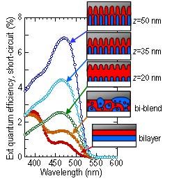
Enhancing the performance of solar cells through controlled heterostructures.
“This discovery paves the way for the next generation of highly-efficient light-emitting diodes and solar cells from organic polymer semiconductor materials,” says Ms Rui-Qi Png, NUS graduate student and lead author of the report.
Using heterostructures as a building block, NUS and Cambridge researchers are now working on projects that could eventually make possible power-efficient large-area lighting films that can be pasted onto tables and walls, and also solar cell films that can be be pasted onto windows.
“Organic polymer semiconductor materials already have the advantage of being easy to deposit using low-temperature additive processing which are inherently energy efficient. Our work brings this one step further to enable new technologies in printable plastic electronics,” adds Prof Peter Ho, principal investigator from the Department of Physics, NUS.
“For this work we went through a number of development cycles of iterative materials chemistry and device work that took us several years,” says Prof Lay-Lay Chua, principal investigator from the Department of Chemistry, NUS. The scientists had to first develop a new approach to photocrosslinking of polymer semiconductors. Although a number of chemistries to do photocrosslinking already existed, none was found entirely satisfactory when applied to polymer semiconductors, due to the stringent demands for high electronic quality in semiconductors. “We took some time to figure out that what was causing issues was the close molecular interaction between the crosslinker and the polymer. Once we have realised this, it set us on a path to finding molecular engineering ways to suppress this interaction. And it worked.”
This breakthrough was developed together with the groups led by Prof Sir Richard Friend, NUS Tan Chin Tuan Centennial Professor and Cavendish Professor at the University of Cambridge, and Dr Jeremy Burroughes, Chief Technology Officer at Cambridge Display Technology. It was partially funded by MOE and A*STAR SERC Thematic Strategic Research Programme on Polymer and Molecular Devices.